
Fig. 1. (a) Tetragonal crystal structure of Sm2Ru3Ge5 as viewed along the c axis. (b) diffraction pattern above and below TCDW showing the CDW peaks. (c) resistivity, (d) heat capacity, (e) Hall coefficient (RH), and (f) electron concentration of Sm2Ru3Ge5.
Charge Density Wave in the New Polymorphs of RE2Ru3Ge5 (RE = Pr, Sm, Dy) and Pb3-ₓSb1+ₓS4Te2- with Square Te sheets en route to superconductivity
CDWs and SDWs have received significant attention from the condensed matter physics and chemistry communities as these broken symmetry ground states are often observed in close proximity to superconductivity. We have focused on exploring materials with charge (CDW) or spin (SDW) density wave to approach superconductivity and uncovered a new polymorph 3D structural family of RE2Ru3Ge5 (RE = Pr, Sm, Dy) and a new 2D phase Pb3SbS4Te2-d that show unique types of CDW.
RE2Ru3Ge5 (RE = Pr, Sm, Dy) crystallize in the 3D tetragonal Sc2Fe3Si5 structure type, Fig. 1. The most striking feature in this compound is CDW order associated with the periodic distortions in the 1D zig-zag Ge chains. In the temperature dependent synchrotron X-ray diffraction data, below 170 K, all peaks are commensurate with the tetragonal lattice, but above 170 K, observed the sudden appearance of additional peaks with respect to the commensurate (hkl) Bragg peaks representing an incommensurate modulation of the parent structure. From X-ray diffraction, charge transport (electrical resistivity, magnetoresistance, Hall effect) and magnetic measurements, and heat capacity, the ordering temperatures (TCDW) observed in the Pr and Sm analogs are ~ 200 K and ~ 175 K, respectively.
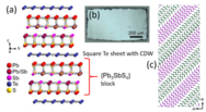
A new 2D phase Pb3SbS4Te2-d has a semiconducting block of [Pb3SbS4]1+ alternating for (Te2)1- square which exhibit vacancies highly sensitive to the cooling rate in synthesis. The compound has an energy gap and the CDW has an incommensurate FS nesting vector of q=0.222a* + 0.223b* + 0.375c*. The transition to the non-CDW state lies above room temperature in the region of ~370 K. The charge transport measurements show that the resistivity is thermal activated from 10 - 370 K as expected from a CDW gap but becomes metallic >370 K.
“Charge Density Wave in the New Layered Compound Pb3-xSb1+xS4Te2-d with Square Te Sheets” H. Chen, C. D. Malliakas, A. Narayan, L. Fang, D. Y. Chung, L. K. Wagner, W.-K. Kwok, and M. G. Kanatzidis J. Am. Chem. Soc. 2017
“Charge Density Wave in the New Polymorphs of RE2Ru3Ge5 (RE = Pr, Sm, Dy)” Bugaris, D. E.; Malliakas, C. D.; Han, F.; Calta, N. P.; Sturza, M.; Krogstad, M.; Osborn, R.; Rosenkranz, S.; Ruff, J.; Trimarchi, G.; Bud’ko, S. L.; Balasubramanian, M.; Chung, D. Y.; Kanatzidis, M. G. J. Amer. Chem. Soc., 2017, 139, 4130-4143. (DOI: 10.1021/jacs.7b00284).