Researchers at the U.S. Department of Energy’s (DOE) Argonne National Laboratory and the University of Chicago have invented an innovative way for different types of quantum technology to “talk” to each other using sound. The study, published Feb. 11 in Nature Physics, is an important step in bringing quantum technology closer to reality.
Researchers are eyeing quantum systems, which tap the quirky behavior of the smallest particles, as the key to a fundamentally new generation of atomic-scale electronics for computation and communication. But a persistent challenge has been transferring information between different types of technology, such as quantum memories and quantum processors.
“We approached this question by asking: Can we manipulate and connect quantum states of matter with sound waves?” said David Awschalom, Argonne senior scientist, Liew Family Professor with the Institute for Molecular Engineering at the University of Chicago, and senior author on the paper.
One way to run a quantum computing operation is to use “spins” — a property of an electron that can be up, down or both. Scientists can use these like zeroes and ones in today’s binary computer programming language. But getting this information elsewhere requires a translator, and scientists thought sound waves could help.
“The object is to couple the sound waves with the spins of electrons in the material,” said graduate student Samuel Whiteley, the co-first author on the paper. “But the first challenge is to get the spins to pay attention.” So they built a system with curved electrodes to concentrate the sound waves, like using a magnifying lens to focus a point of light.
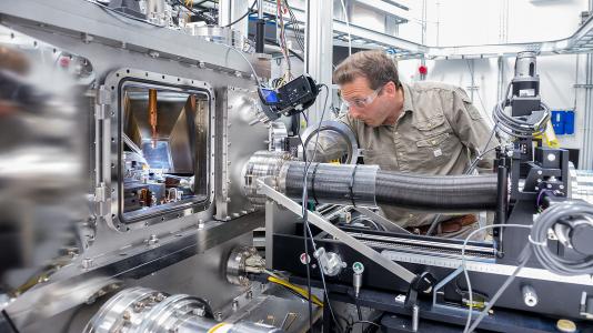
The results were promising, but they needed more data. To get a better look at what was happening, they worked with scientists at the Center for Nanoscale Materials, a DOE Office of Science User Facility at Argonne, to observe the system in real time. Essentially, they used extremely bright, powerful X-rays from the lab’s synchrotron, the Advanced Photon Source, also a DOE Office of Science User Facility, as a microscope to peer at the atoms inside the material as the sound waves moved through it at nearly 7,000 kilometers per second.
“This new method allows us to observe the atomic dynamics and structure in quantum materials at extremely small length scales,” said Awschalom. “This is one of only a few locations worldwide with the instrumentation to directly watch atoms move in a lattice as sound waves passes through them.”
One of the many surprising results, the researchers said, was that the quantum effects of sound waves were more complicated than they’d first imagined. To build a comprehensive theory behind what they were observing at the subatomic level, they turned to Prof. Giulia Galli, the Liew Family Professor at UChicago’s IME and a senior scientist at Argonne. Modeling the system involves marshalling the interactions of every single particle in the system, which grows exponentially, Awschalom said, “but Professor Galli is a world expert in taking this kind of challenging problem and interpreting the underlying physics, which allowed us to further improve the system.”
It’s normally difficult to send quantum information for more than a few microns, said Whiteley — that’s the width of a single strand of spider silk. This technique could extend control across an entire chip or wafer.
“The results gave us new ways to control our systems, and opens venues of research and technological applications such as quantum sensing,” said postdoctoral researcher Gary Wolfowicz, the other co-first author of the study.
The discovery is another from the University of Chicago’s world-leading program in quantum information science and engineering; Awschalom is currently leading a project to build a quantum “teleportation” network between Argonne and Fermi National Accelerator Laboratory to test principles for a potentially unhackable communications system.
The scientists pointed to the confluence of expertise, resources and facilities at the University of Chicago, Institute for Molecular Engineering and Argonne as key to fully exploring the technology.
“No one group has the ability to explore these complex quantum systems and solve this class of problems; it takes state-of-the-art facilities, theorists and experimentalists working in close collaboration,” Awschalom said. “The strong connection between Argonne and the University of Chicago enables our students to address some of the most challenging questions in this rapidly moving area of science and technology.”
Other coauthors on the paper are UChicago Assoc. Prof. David Schuster, UChicago Prof. and Argonne Senior Scientist Andrew Cleland; Argonne National Laboratory scientists Joseph Heremans and Martin Holt; graduate students Christopher Anderson, Alexandre Bourassa, He Ma and Kevin Satzinger; and postdoctoral researcher Meng Ye.
The devices were fabricated in the Pritzker Nanofabrication Facility at the William Eckhardt Research Center. Materials characterization was performed at the UChicago Materials Research Science and Engineering Center. The scanning microscopy that took X-ray images of the acoustic wave were performed on the Hard X-ray Nanoprobe at the Center for Nanoscale Materials and Advanced Photon Source.
Funding was provided by the Air Force Office of Scientific Research, the U.S. Department of Energy Office of Basic Energy Sciences, the National Science Foundation, and the U.S. Department of Defense.
The Center for Nanoscale Materials is one of the five DOE Nanoscale Science Research Centers, premier national user facilities for interdisciplinary research at the nanoscale supported by the DOE Office of Science. Together the NSRCs comprise a suite of complementary facilities that provide researchers with state-of-the-art capabilities to fabricate, process, characterize and model nanoscale materials, and constitute the largest infrastructure investment of the National Nanotechnology Initiative. The NSRCs are located at DOE’s Argonne, Brookhaven, Lawrence Berkeley, Oak Ridge, Sandia and Los Alamos National Laboratories. For more information about the DOE NSRCs, please visit https://science.energy.gov/bes/suf/user-facilities/nanoscale-science-research-centers/.
Argonne National Laboratory seeks solutions to pressing national problems in science and technology by conducting leading-edge basic and applied research in virtually every scientific discipline. Argonne is managed by UChicago Argonne, LLC for the U.S. Department of Energy’s Office of Science.
The U.S. Department of Energy’s Office of Science is the single largest supporter of basic research in the physical sciences in the United States and is working to address some of the most pressing challenges of our time. For more information, visit https://energy.gov/science.

