By keeping ferroelectric ‘bubbles’ intact, researchers pave way for new devices
When a magician suddenly pulls a tablecloth off a table laden with plates and glasses, there is a moment of suspense as the audience wonders if the stage will soon be littered with broken glass. Until now, an analogous dilemma had faced scientists working with special electrical bubbles to create the next generation of flexible microelectronic and energy storage devices.
Scientists at the U.S. Department of Energy’s (DOE) Argonne National Laboratory have discovered a new way to do an atomic-scale version of the tablecloth trick by peeling off heterostructure thin films containing electrical bubbles from a particular underlying material, or substrate, while keeping them fully intact. The discovery may bring us one step closer to a host of applications that rely upon these unusual and brittle structures.
“You can think of it like trying to remove a house from its foundation. Normally, you would think that the house would collapse, but we found that it retained all of its properties.” – Saidur Bakaul, Argonne materials scientist
“The bubbles are very fragile and initially need particular underlying materials, called substrates, and specific conditions in order to grow films with them in,” said Argonne materials scientist Saidur Bakaul. “There are many materials of interest to us for which these bubbles could be extremely useful, like plastics. However, we haven’t been able to grow them directly on these materials. Our research is the initial step to make bubbles possible there.”
The electric bubbles are found in a three-layer ultrathin structure with alternating electrical properties: ferroelectric, then dielectric, then ferroelectric again. The bubbles in this multilayer structure are made out of specially ordered dipoles, or twinned electric charges. The orientation of these dipoles is based on the local strain in the material and charges on the surface which cause the dipoles to seek out their relative lowest energy state. Eventually, the electric bubbles (bubble domains) form but only when certain conditions are met. They are also easily distorted by even small forces.
In the experiment, Bakaul’s colleagues at University of New South Wales first grew the bubbles in an ultrathin heterostructure film on a strontium titanate substrate — one of the easiest materials on which to create them. Then, Bakaul faced the challenge of removing the heterostructure from the substrate while retaining the bubbles. “You can think of it like trying to remove a house from its foundation,” he said. “Normally, you would think that the house would collapse, but we found that it retained all of its properties.”
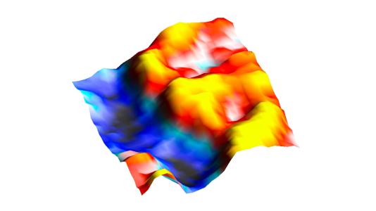
Bubble domains are tiny. They’re only about 4 nanometers in radius — just as wide as a human DNA strand. Therefore, they are difficult to see. In Argonne’s Materials Science division, advanced scanning probe microscopy techniques with Fourier transform analysis allow scientists to not only see them but also quantify their properties in the freestanding films.
To establish that the bubble domains remained intact, Bakaul measured their electronic (capacitance) and piezoelectric properties through two microscopy techniques: scanning microwave impedance microscopy and piezoresponse force microscopy. If the bubbles had disintegrated, the capacitance would have changed under an applied voltage, but Bakaul saw that it stayed relatively stable up to a fairly high voltage.
These experiments validated numerical estimations of capacitance obtained from theoretical analyses that Bakaul and his student developed by combining atomistic simulations with circuit theory. “The combination of experiment and simulation proved conclusively that these bubbles are capable of living even when removed from the original substrate. That was something we had hoped to achieve for a long time,” Bakaul said.
When the bubbles were removed, the heterostructure film — which previously lay flat like a tablecloth — suddenly assumed a rippled appearance. While Bakaul noted that many might assume this change would impair the bubbles’ properties, he found that the bubbles were actually protected by a change in the materials’ built-in voltage. Atomistic simulations done by Bakaul’s colleagues at the University of Arkansas suggested that the elastic energy at the free interfaces is the origin of the ripple formation.
The result is exciting, according to Bakaul, because these bubbles have unusual and intriguing electrical and mechanical properties. “Ferroelectric bubbles are newly discovered nanoscale objects,” he said. “There is a consensus in the community that they may have a lot of applications. For instance, transformation of these bubbles results in an unusually high electromechanical response, which can have applications in a wide range of devices in microelectronics and energy applications.”
Although it’s physics and not magic that has created a potential new avenue for the integration of these bubbles, Bakaul indicated that new technologies based on them could have a transformative impact. “Whether we’re discussing energy harvesters or supercomputers, these bubbles could make a big difference for many different materials and applications,” he said.
The research was funded by the DOE’s Office of Science (Office of Basic Energy Sciences). The authors leveraged nanofabrication and cleanroom facilities at Argonne’s Center for Nanoscale Materials, a DOE Office of Science user facility, to prepare samples for electrical characterization.
A paper based on the research, “Freestanding Ferroelectric Bubble Domains,” was published in the September 19 issue of Advanced Materials. Other authors of the paper include Argonne’s Amanda Petford-Long, as well as Sergei Prokhorenko, Yousra Nahas and Laurent Bellaiche of the University of Arkansas, plus Qi Zhang and Nagarajan Valanoor of the University of New South Wales and Yushi Hu of the University of Chicago (intern student at Argonne).
About Argonne’s Center for Nanoscale Materials
The Center for Nanoscale Materials is one of the five DOE Nanoscale Science Research Centers, premier national user facilities for interdisciplinary research at the nanoscale supported by the DOE Office of Science. Together the NSRCs comprise a suite of complementary facilities that provide researchers with state-of-the-art capabilities to fabricate, process, characterize and model nanoscale materials, and constitute the largest infrastructure investment of the National Nanotechnology Initiative. The NSRCs are located at DOE’s Argonne, Brookhaven, Lawrence Berkeley, Oak Ridge, Sandia and Los Alamos National Laboratories. For more information about the DOE NSRCs, please visit https://science.osti.gov/User-Facilities/User-Facilities-at-a-Glance.
Argonne National Laboratory seeks solutions to pressing national problems in science and technology by conducting leading-edge basic and applied research in virtually every scientific discipline. Argonne is managed by UChicago Argonne, LLC for the U.S. Department of Energy’s Office of Science.
The U.S. Department of Energy’s Office of Science is the single largest supporter of basic research in the physical sciences in the United States and is working to address some of the most pressing challenges of our time. For more information, visit https://energy.gov/science.