
University of Missouri researchers use Advanced Photon Source to characterize semiconductor material potentially useful for solar cells

Researchers from the University of Missouri, in collaboration with scientists from the University of Western Cape in South Africa and physicists at the U.S. Department of Energy’s (DOE) Argonne National Laboratory, have developed a new way to make hybrid perovskites — a combination of organic and inorganic semiconducting materials — that could form the basis of new solar cells or other electronic devices.
University of Missouri physicist Suchismita (Suchi) Guha and her collaborators improved the methods for making lead halide perovskites. Previous techniques for making these thin-film perovskites required liquid processing using solvents, which rendered the perovskite films susceptible to degradation when exposed to air. Additionally, with this prior manufacturing process, part of the perovskite undergoes a temperature-dependent phase change to its structure, causing performance limitations in real-world operating conditions.
With the new technique, which paired chemical vapor deposition (CVD) with an additional step using a chloride ion, the researchers were able to prevent the phase change in the perovskite, holding it in a stable structure throughout a large temperature range. Additionally, the CVD technique rendered the perovskite air stable, making it appropriate for a potential solar cell.
The structure of the perovskite was analyzed at Argonne’s Advanced Photon Source.
Argonne partners with Washington University in St. Louis to deconstruct how photosynthesis works

Scientists have long sought to understand photosynthesis, the process by which plants and other organisms use the sun’s energy to create their own food. In a breakthrough discovery, researchers from the DOE Argonne National Laboratory and Washington University in St. Louis have detected how modified photosynthetic proteins capture light and use it to initiate a series of electron transfer reactions.
Scientists traced the movement of electrons to discover how work is accomplished inside the cell of a photosynthetic organism. After a plant absorbs sunlight, electrons normally take only one of two possible pathways. Scientists engineered a protein complex to disable one pathway and enable the other, changing the electron’s direction. The team’s findings move science closer to harnessing the flow of energy — a feat that promises to greatly enhance the efficiency of many solar-powered devices, including solar panels and sensors.
The DOE Office of Science sponsored this research.
Aerospace team harnesses the power of supercomputers to study aircraft drag

In flight, airplanes experience a resistive drag that slows their motion and requires great amounts of fuel to overcome. For long-haul aircraft — planes designed for 6- to 12-hour flights — this friction accounts for about half the total drag. Reducing drag promises to slash the amount of fuel required and limit the environmental impact. Researchers at the Missouri University of Science and Technology and NASA’s Langley Research Center in Hampton, Virginia used supercomputers at the Argonne Leadership Computing Facility (ALCF) to study drag.
Drag is caused by friction between the plane’s surface and the air. For shapes like airplane wings, the effects of friction are confined to the boundary layer, a thin region near the wing’s surface. The resistive force associated with the boundary layer is relatively modest when fluid motion is regular and ordered, but becomes chaotic at high speeds because of turbulent motion.
The study focused on the backward-angling swept-wings similar to those on most aircraft and whose dynamics are difficult to predict and control. Using high-performance computing, the team conducted petascale simulations of the entire process. Their findings may impact the design of many devices besides aircraft, such as wind turbines.
The ALCF is a DOE Office of Science User facility.
Argonne, MU partner on novel technique to advance how semiconductors are made
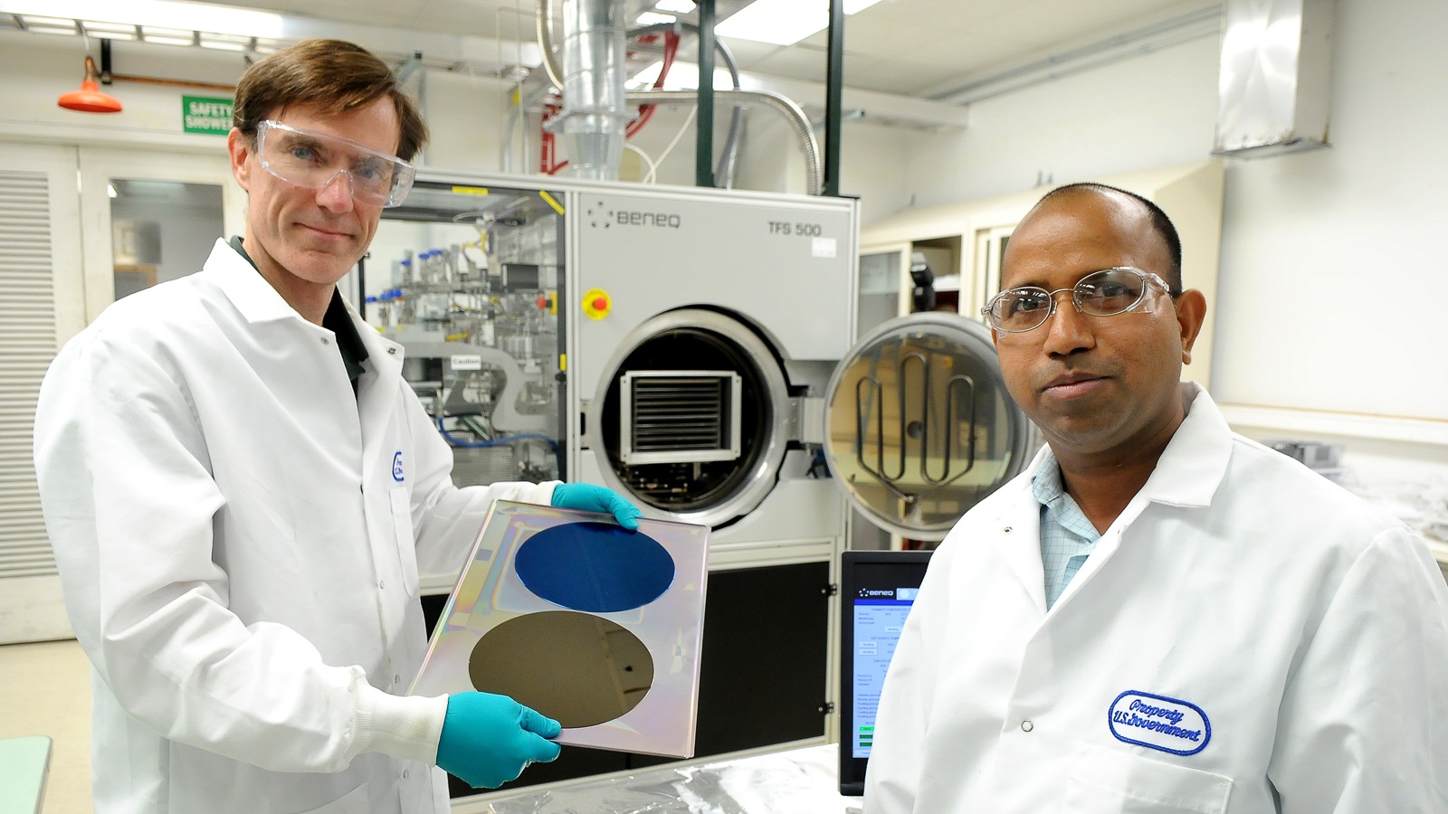
Argonne and a team led by Matthias Young at MU have developed a new technique that could pack more circuitry onto semiconductors, increasing the speed and capability of computers. Known as molecular layer etching (MLE), the technique promises to usher in new pathways for fabricating materials at nanoscale.
Microelectronics like semiconductor devices are at the heart of the technologies we use each day. To make them smaller and faster, manufacturers cram in more and more circuitry onto films and 3D structures. Today, this happens by using thin film deposition and etching to grow or remove films one layer at a time.
MLE can be used to design microscopic architectures, enabling manufacturers and researchers to develop new ways of making nanostructures. The process may also be a safer option because it is free of halogens, the harsh components of chemicals common in other etching processes.
This research was funded by the Center for Electrochemical Energy Science, an Energy Frontier Research Center supported by DOE’s Office of Science.